Search models, users, collections, and posts

CMOS 3NAND Logic Semiconductor Design
IP Report
Print Profile(1)
0.16mm layer, 2 walls, 15% infill
Designer
4 h
1 plate
Open in Bambu Studio
Boost
2
10
0
0
6
2
Released
Description
Content has been automatically translated.
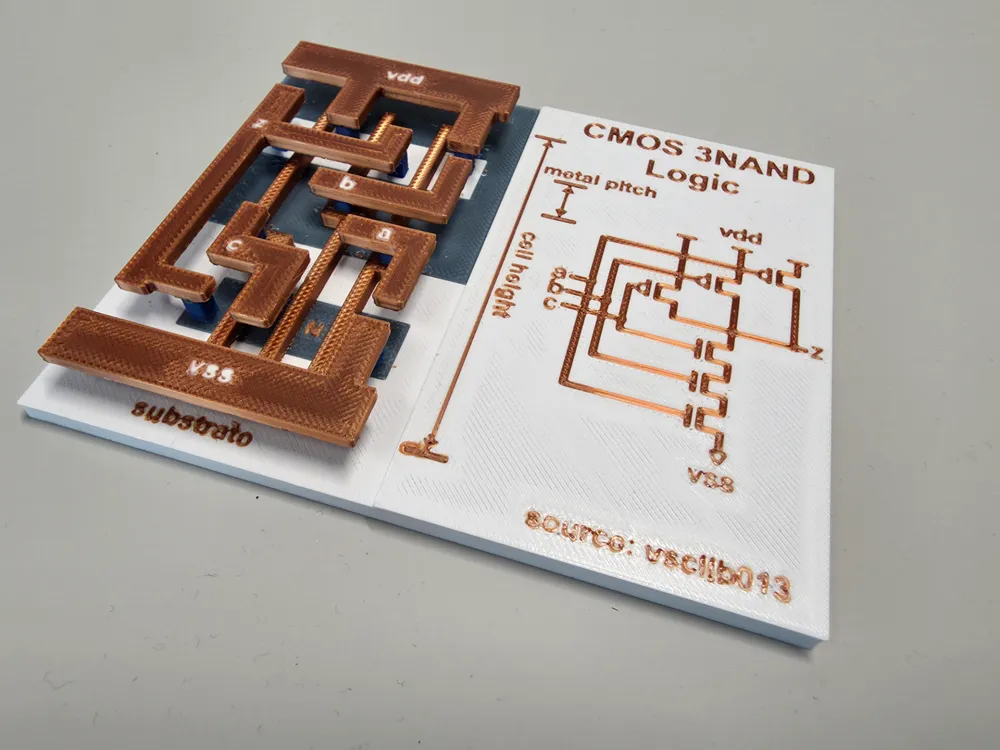
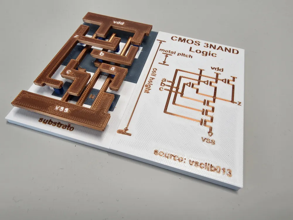
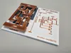
Model of a Logic Semiconductor Layout. This layout corresponds to a 3-NAND (NOT AND) design with 6 transistors. The source is indicated in the design
Supports are a bit annoying to remove. One could also print it half and half and glue it together. That should be easy to implement with the 3fm file
License

This user content is licensed under a Standard Digital File License.
You shall not share, sub-license, sell, rent, host, transfer, or distribute in any way the digital or 3D printed versions of this object, nor any other derivative work of this object in its digital or physical format (including - but not limited to - remixes of this object, and hosting on other digital platforms). The objects may not be used without permission in any way whatsoever in which you charge money, or collect fees.


Comment & Rating (0)