
TO-220 Transistor Lead Forming Tool
Print Profile(1)
Description
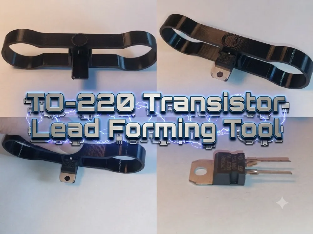
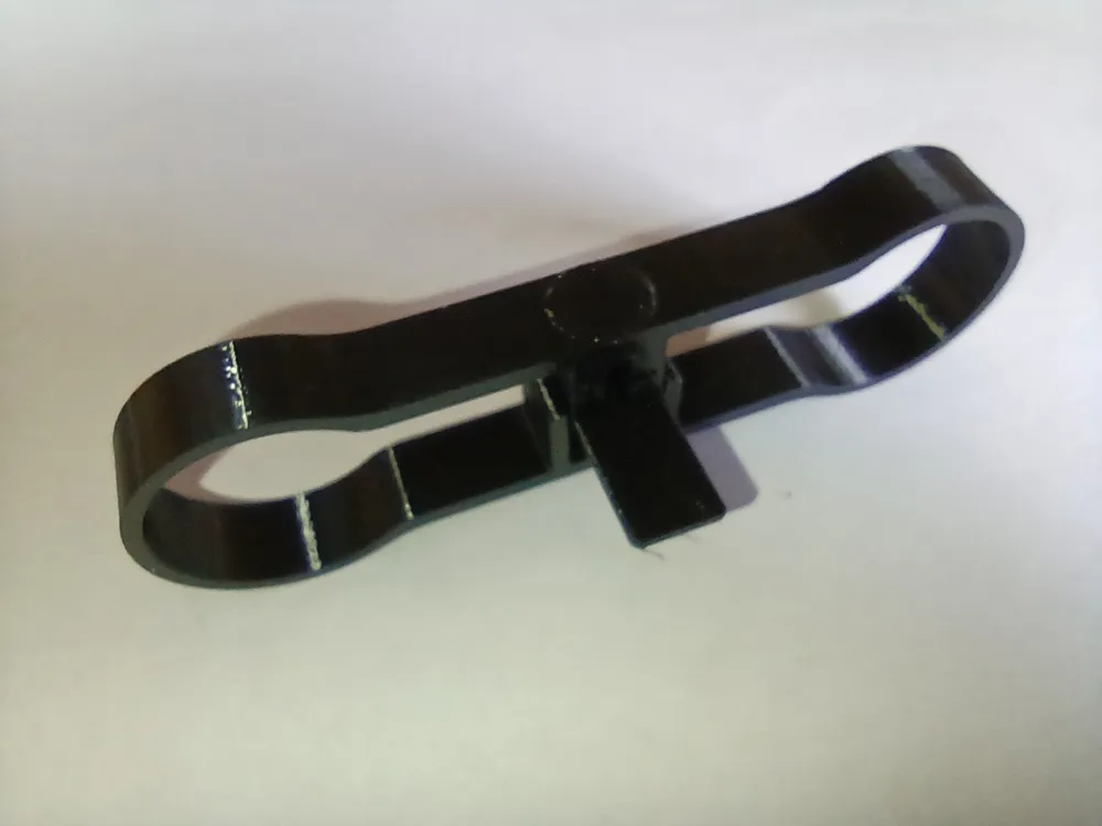
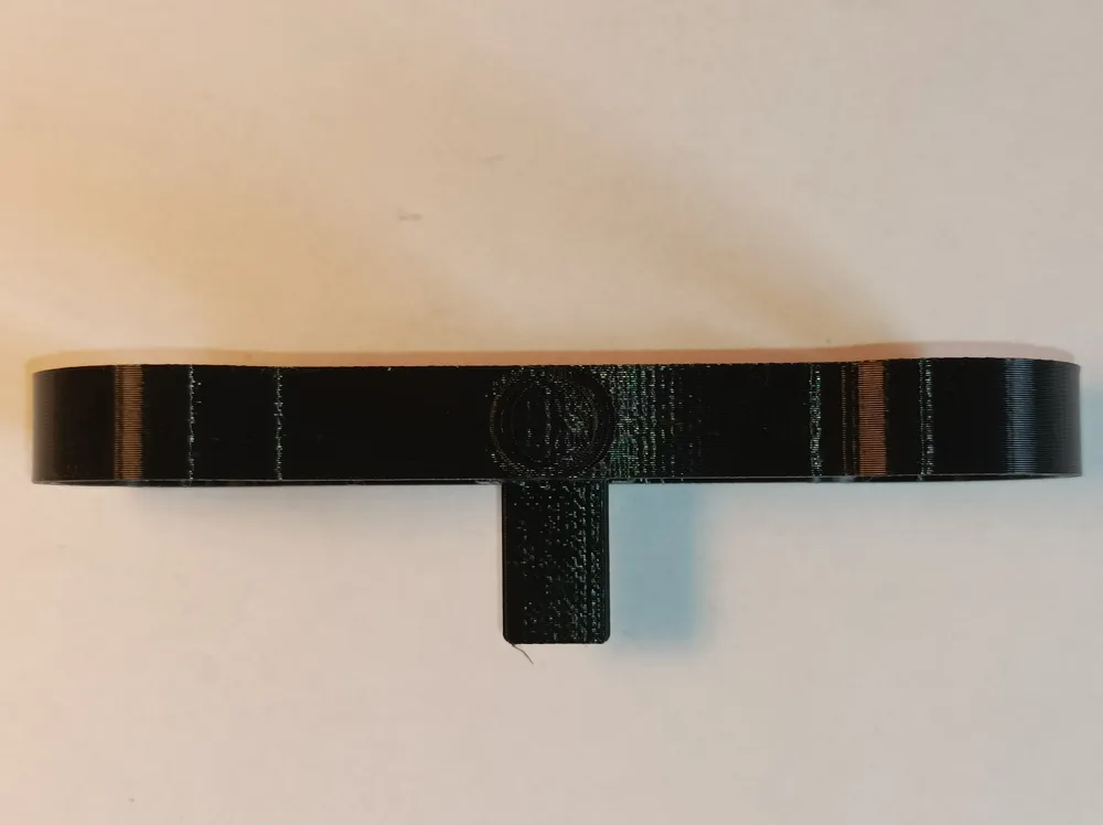
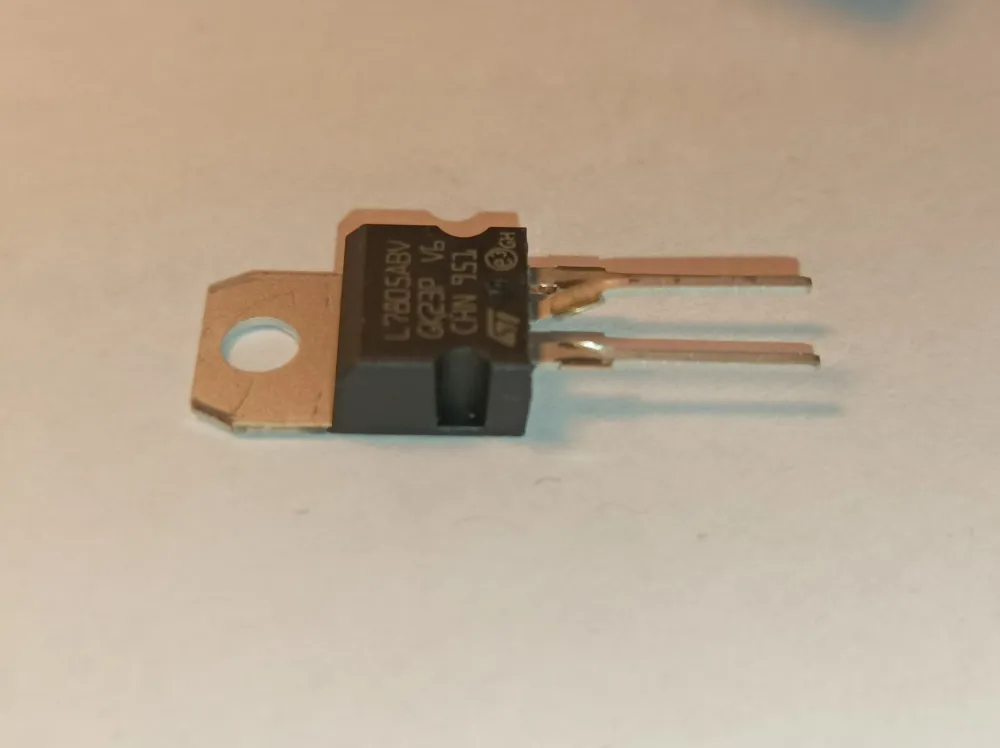
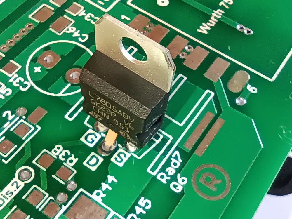
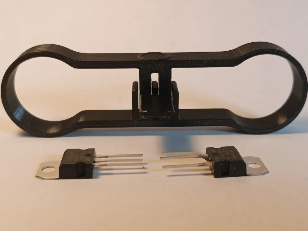
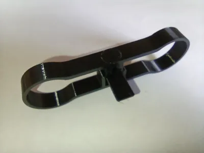
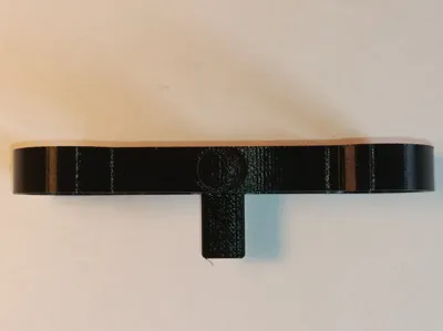
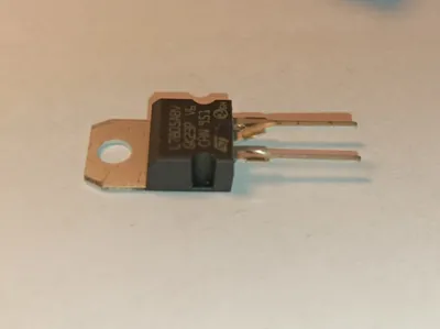
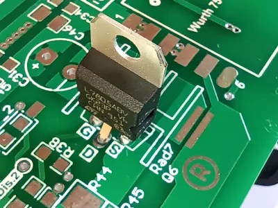
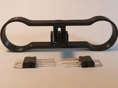
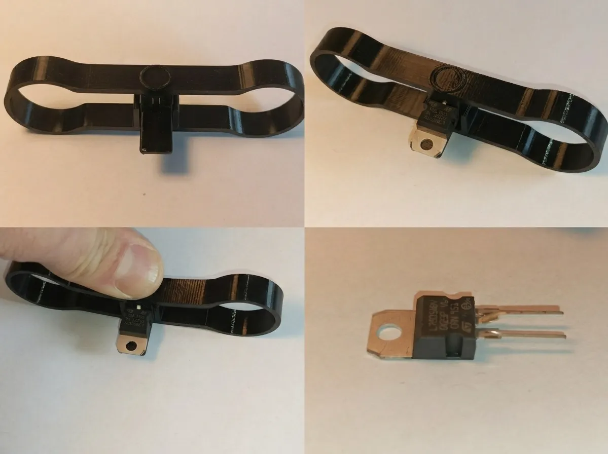
This tool was designed to easily bend/form the center lead of TO-220 transistors for PCB designs that require a 2.5 mm center pin offset.
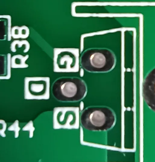
I have personally processed hundreds of transistors with this jig. The bending process is completely effortless, quick, and highly repeatable, ensuring identical results every single time.
Quick Instructions:
- Insert the transistor.
- Squeeze.
...and you're done!
Print Settings:
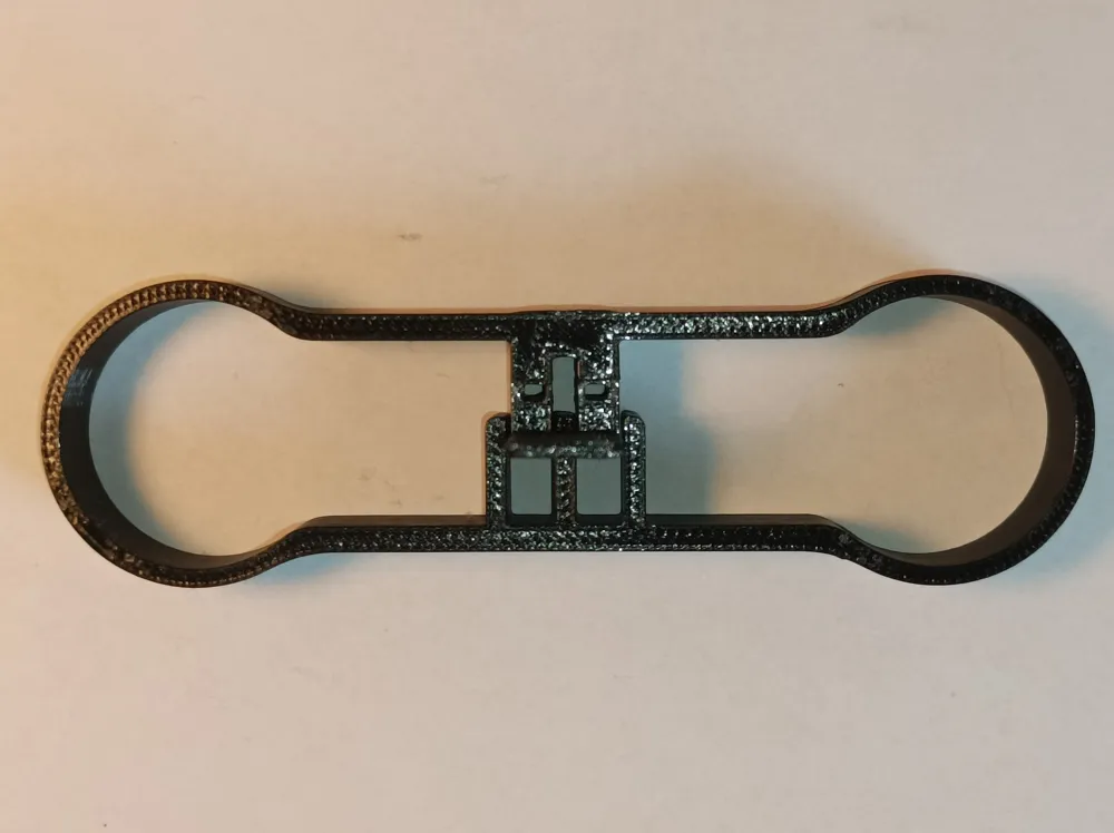
- Material: PETG recommended (for optimal flexibility and durability of the spring mechanism).
- Supports: None required.
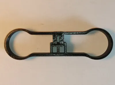
- Infill: 100% (Solid infill is highly recommended and tested).
Filament usage: ~7.6 grams.
License

You may create derivative works based on this object, provided that all such derivative works are published exclusively on the MakerWorld platform and include proper attribution to the original creator. You may not share, upload, host, distribute, or publish this object—or any derivative work of this object—on any other digital platform, marketplace, or distribution channel. Commercial use of this object and any derivative works is strictly prohibited. This includes, but is not limited to, selling, renting, sublicensing, or using the object in any context in which you receive monetary compensation or other financial benefits.


Comment & Rating (0)